- Home
- Users & Science
- Scientific Documentation
- ESRF Highlights
- ESRF Highlights 2017
- Matter at extremes
- Si-III synthesis and characterisation
Si-III synthesis and characterisation
Si-III was found to be a narrow-gap semiconductor following its high-pressure synthesis using the large-volume press at beamline ID06. The complete optical, electronic and thermal transport properties of Si-III have been determined.
Silicon is important for electronics, solar energy conversion and other technological applications. Its capacity to introduce new and unexpected physical phenomena, due to the numerous crystal structures, remains very promising for the development of future advanced applications.
The common structure of Si, called “number I” or Si-I, is that of diamond. High pressure allows new structures to be obtained and then recovered as metastable states under ambient conditions. The large-volume synthesis using both in situ and ex situ methods under high pressures of 7-13 GPa [1] and subsequent characterisation by diverse methods (optical and transport properties) combined with ab initio simulations allowed the Si-III (BC8 structure) to be unambiguously established as a semiconductor with a narrow direct band gap of ~30 meV, contrary to previous theories about its semi-metallic properties.
Metals are able to conduct free electrons, while insulators do not conduct electricity. Semiconductors, employed for electronics, can have their conductivity switched on and off, which is a very useful property. This is due to the ability of their electrons to pass from insulating states (valence band) to conductive states with higher energies (conduction band), by absorbing external energy (thermal, photons). The required energy for such transition is called the band gap energy.
Silicon with diamond structure is a semiconductor, while most high-pressure phases are metallic (e.g. Si-II with β-Sn structure). On decompression of high-pressure forms, one obtains metastable Si-III rather than stable Si-I (Figure 32). The electronic properties of Si-III were controversial until quite recently. Earlier experimental and theoretical results suggested that Si-III is a semi-metal – with a reduced number of free electrons – without any band gap. However, phase-pure samples of sufficient size were not available for characterisation (electrical, thermal, photons).
 |
|
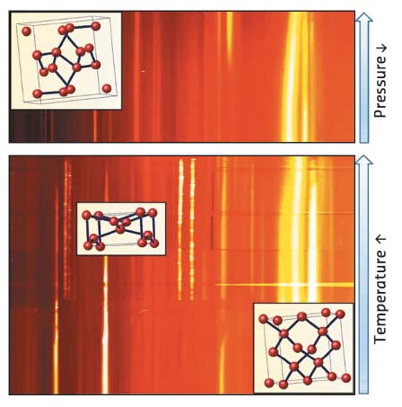
Fig. 32: Metastable silicon allotrope, Si-III, crystallises not only during decompression of the metallic Si-II allotrope with the β-tin structure stable at pressures above 10 GPa (top panel), but also forms during phase transformations as a function of temperature in Na-Si system at remarkably lower pressures, down to 7 GPa (bottom panel). |
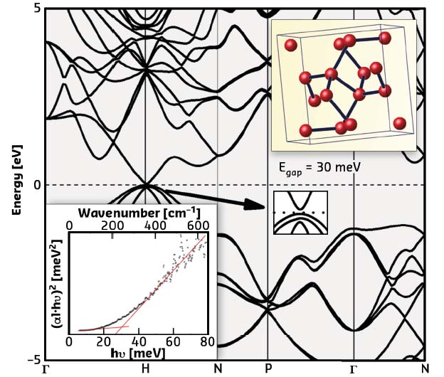
The synthesis of pure Si-III using the large-volume press at beamline ID06 allowed this phase to be established as a semiconductor with an extremely narrow band gap of ~30 meV, 40 times narrower than that of crystals of common Si-I (Figure 33). The formation of the free charge carriers (electrons) is possible by thermal activation, just like classical semiconductors. No free electrons have been observed in the 0 K limit (by heat capacity measurements). The opaque sample becomes transparent to far-infrared photons with energies lower than 30 meV (photon transmission measurements). Ab initio simulations allowed an accurate description of the band structure using the HSE06 hybrid functional, with levels of exact Hartree-Fock exchange mixing above 25% (an approximation more appropriate for systems with free electrons as compared to classical DFT/GW methods).
 |
|
Fig. 33: Electronic structure of Si-III. Insets present the crystalline structure (upper) and the infra-red photon absorption spectra (lower). |
These results show that Si-III can be used beyond the traditional applications of Si where narrow gap semiconductors are used, for example, in infrared photonics, as well as the phenomena of tunnelling and confinement where heavy metal compounds are now used.
Principal publication and authors
BC8 Silicon (Si-III) is a narrow-gap semiconductor, H. Zhang (a), H. Liu (a), K. Wei (b), O.O. Kurakevych (c), Y. Le Godec (c), Z. Liu (a), J. Martin (d), M. Guerrette (a), G.S. Nolas (b) and T.A. Strobel (a), Phys. Rev. Lett. 118, 146601 (2017); doi: 10.1103/PhysRevLett.118.146601.
(a) Geophysical Laboratory, Carnegie Institution of Washington, Washington DC (USA)
(b) Department of Physics, University of South Florida, Tampa (USA)
(c) IMPMC, UPMC Sorbonne Universités, UMR CNRS 7590, Muséum National d’Histoire Naturelle, IRD UMR 206, Paris (France)
(d) Material Measurement Laboratory, National Institute of Standards and Technology, Gaithersburg, Maryland (USA)
References
[1] O.O. Kurakevych et al., Inorg. Chem. 55, 8943-8950 (2016)
partners


European Synchrotron Radiation Facility - 71, avenue des Martyrs, CS 40220, 38043 Grenoble Cedex 9, France.