- Home
- Users & Science
- Scientific Documentation
- ESRF Highlights
- ESRF Highlights 2000
- Applied and Industrial Research
- ID27 - An Industrial SR-TXRF Facility Opens its Doors to the Semiconductor Community
ID27 - An Industrial SR-TXRF Facility Opens its Doors to the Semiconductor Community
Metallic contaminants at the surface of silicon wafers can greatly hinder the performance of integrated circuits. The present IC technology of 0.25 µm feature sizes on 200 mm wafers can tolerate transition element contaminant concentrations between 2 and 5 x 10¹⁰ atoms/cm2 which requires minimum surface detection limits between 2 and 5 x 10⁹ atoms/cm2. At this level of detection the existing non-destructive method for measuring metallic surface contamination, Total Reflection X-ray Fluorescence (TXRF) using conventional laboratory X-ray sources, is approaching its limits.
The use of synchrotron radiation rather than the isotropic emission of laboratory sources presents numerous advantages for TXRF, ranging from increased photon intensity and highly collimated beams, to flexible energy tunability and a high degree of linear polarisation. The benefits that can be reaped are improved detection limits, low Z element detection, reduced measuring time, mapping capabilities and depth profiling.
The project to construct a dedicated industrial SR-TXRF instrument at the ESRF on ID27 was launched in July 1997 and was financed by the ESRF, CEA/LETI and France Télécom/CNET and the European MEDEA programme (Micro-Electronics Development for European Applications).
The facility is equipped with an aperiodic undulator, a fixed-exit silicon (111) channel-cut monochromator, a multilayer monochromator and a harmonic rejection mirror. The end-station is in a class 100 laminar flow enclosure, located in a shielded hutch of about 25 m2. It encompasses a loading robot that transfers the wafers from standard cassettes to a load-lock vessel, a high vacuum handler that transfers the wafers from the interlock loading chamber to the measuring position in the main TXRF chamber, two single-element Si(Li) detectors (which are now being replaced by definitive multi-element array detectors) for the parallel acquisition of the fluorescence spectra, and a wafer chuck/manipulator for positioning the wafer in the X-ray beam and rotating the wafer in order to perform the mapping of contamination over the entire wafer surface. The loading, unloading and pumping down of wafers is completely automated. The system is designed to accomodate both 200 and 300 mm wafers.
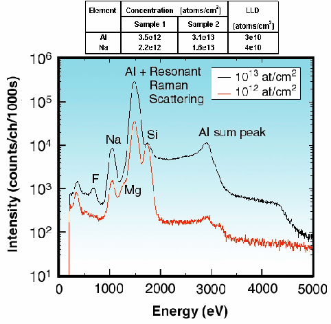 |
Fig. 124: Fluorescence spectra recorded from two standard wafers intentionally contaminated with Al and Na in the 10 12 and 10 13 atoms/cm 2 range. The primary photon energy was 1670 eV; the elastic scattering peak is highly attenuated due to the detection geometry and the polarisation of the beam. The measured concentrations and the lower limits of detection (LLD) are given in the inset table.
|
The beamline was fully constructed by spring 2000 and started its commissioning phase in collaboration with industrial partners. The results obtained were extremely promising. The analyses currently being carried out have achieved lower limits of detection (LLD) of around 5.108 atoms/cm2 for transition elements and 5.1010 atoms/cm2 for low Z elements (Al, Mg, Na) as shown in Figure 124. The first new six-element linear array of Si(Li) detectors, optimised for wafer mapping, was installed in November and a second should be operational in spring 2001, which will enable us to push these LLDs even further. The full operation régime will be reached at the beginning of 2001.
Authors
G. Apostolo, R. Barrett, M. Robichon, M. Navizet and F. Comin.
ESRF
partners


European Synchrotron Radiation Facility - 71, avenue des Martyrs, CS 40220, 38043 Grenoble Cedex 9, France.