- Home
- Users & Science
- Scientific Documentation
- ESRF Highlights
- ESRF Highlights 2015
- X-ray nanoprobe
- Probing nanowires in the spatial and time domains
Probing nanowires in the spatial and time domains
An imaging tool to investigate nanowires with site, optical and chemical sensitivity has been developed using pulsed hard X-ray nanobeams. Its unprecedented temporal and spatial resolution provided a deeper understanding of geometrical size-dependent phenomena. The approach opens new avenues for further imaging studies in nanoscience.
Interest in semiconductor nanowires for nanoscale devices has been greatly driven by their simultaneous capability of optical guiding and electrical driving, and large surface to volume ratio, which is crucial for sensitive and selective sensors. Although it is rather difficult to find single analytical tools covering simultaneously several properties in the length and time scales, most nanowire applications rely on the ability not only to grow, but also to fully characterise individual and collections of nanowires. Accordingly, synchrotron based nanoprobes in the multi-keV energy range have great potential in terms of surface/deep information depths, element-, site-, and orbital-selectivity, structural and chemical trace sensitivity, as well as temporal effects.
Examples of the use of hard X-ray nanobeams at beamline ID22 in the determination of spatially-resolved properties of nanowires by concurrent X-ray fluorescence (XRF), X-ray absorption, and/or X-ray diffraction include the investigation of the ion implantation process in a possible formation of magnetic precipitates in single ZnO nanowires [1], the spontaneous phase segregation in single InxGa1–xN nanowires [2], local order in crossed Ga2O3/SnO2 wires [3], as well as the controlled epitaxy of core-multishell InGaN/GaN multiquantum well wires [4].
As an illustration, here we show how a hard X-ray nanoprobe was used for the first time to examine geometrical quantum confinement within a single coaxial nanowire based light emitting diode. Owing to its central role in limiting carrier dynamics, the specific use of the X-ray excited optical luminescence (XEOL) technique allows the optical imaging of nanosized-dependent dynamics in core-multishell nanowires.
 |
|
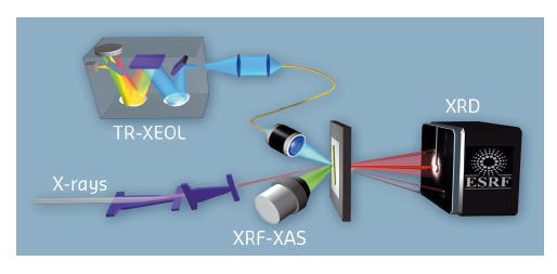
Fig. 18: Multimodal setup at the former nanoprobe beamline ID22 (now at ID16B). |
Figure 18 shows a schematic of the ID22 nanoprobe (now at ID16B) that provides simultaneous compositional, structural, and optical information with high spatio-temporal resolution. Apart from the emission of characteristic secondary X-rays collected with a Si drift detector, while raster-scanning the sample, the X-ray diffraction patterns can be recorded with a FReLoN camera, and the emitted photons detected by a far-field optical system. As a proof of concept, the XEOL approach has been applied to hexagonal n-GaN/InxGa1–xN/n-GaN nanowire based light emitting diodes. XRF analyses (not shown) revealed that the radial chemical composition is consistent with the targeted heterostructure design. After the X-ray absorption process, an electron is promoted to a high energy state above the Fermi level, leaving behind a hole in the core shell. Both carriers relax their energy mostly by emission of photons (XRF), electrons, and lower energy phonons until they find their corresponding band minima near the semiconductor band gap energy (typically 0.5-3 eV). The XEOL signal arises from the radiative recombination of these thermalised electron hole pairs that have a characteristic decay time ranging from a few tens picoseconds to a few tens of nanoseconds depending on their spatial overlap.
 |
|
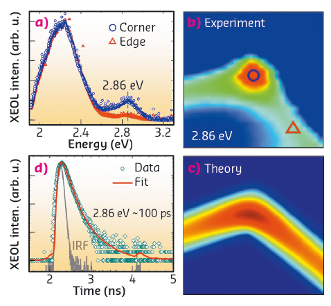
Fig. 19: (a) XEOL spectra acquired at the corner and at the edge of the hexagonal core-multishell nanowire. (b) XEOL intensity map of the emission at 2.86 eV (1.8 x 1.8 µm2). (c) Electron probability density calculated for the same structure. (d) Time-resolved XEOL decay curve recorded for the 2.86 eV band at the hexagon corner. |
Figure 19 displays different results for an InxGa1–xN/GaN core-multishell nanowire by scanning a 60 x 60 nm2 X-ray spot across its radial direction. The spectra shown in Figure 19a have been taken at the edge and the corner of the hexagon, respectively. In both cases, two emission bands can be identified: a broad band at 2.21 eV attributed to the common yellow band, which has the largest excited volume, and a narrower band at 2.86 eV attributed to the transitions from the InGaN/GaN multiquantum wells. Figure 19b displays the spatial projection of the luminescence intensity at 2.86 eV. The multiquantum wells signal appears confined to the edges of the nanowire, revealing intensity maxima at the hexagon corners. Theoretical calculations indicate that geometrical quantum confinement might be responsible for this effect. The square of the electron wave function in its ground state is depicted in Figure 19c. The wave function for the electrons in its lowest energy state, and similarly for the holes (not shown), is localised at the corner, decaying towards the edges of the hexagon. Figure 19d shows the fast luminescence decay curve of the multiquantum wells emission measured at the hexagon corner. Using the 16-bunch filling mode of the storage ring [5.68 MHz repetition frequency and 50 ps pulse duration], time-resolved-XEOL data could also be simultaneously collected with the X-ray nanoprobe. The decay time of 100 ps clearly supports the ultrafast recombination processes related to the intriguing quantum confinement size effects as well.
Principal publication and authors
Exploring single semiconductor nanowires with a multimodal hard X-ray nanoprobe, G. Martínez-Criado (a), J. Segura-Ruiz (a), B. Alén (b), J. Eymery (c), A. Rogalev (a), R. Tucoulou (a) and A. Homs (a), Advanced Materials 26, 7873-7879 (2014); doi: 10.1002/adma.201304345.
(a) ESRF
(b) IMM-Instituto de Microelectrónica de Madrid (CNM-CSIC), Tres Cantos (Spain)
(c) Equipe mixte CEA-CNRS-UJF “Nanophysique et semiconducteurs”, SP2M, UMR-E CEA/UJF-Grenoble 1, INAC, Grenoble (France)
References
[1] J. Segura-Ruíz et al., Nano Letters 11, 5322 (2011).
[2] J. Segura-Ruíz et al., Nano Letters 14, 1300 (2014).
[3] G. Martínez-Criado et al., Nano Letters 14, 5479 (2014).
[4] G. Martínez-Criado et al., Nano Letters 12, 5829 (2012).
partners


European Synchrotron Radiation Facility - 71, avenue des Martyrs, CS 40220, 38043 Grenoble Cedex 9, France.