- Home
- Users & Science
- Scientific Documentation
- ESRF Highlights
- ESRF Highlights 2004
- Surface and Interface Science
- Ion Beam Induced Ripple Structure of Crystalline Layers in Si Wafers
Ion Beam Induced Ripple Structure of Crystalline Layers in Si Wafers
The formation of a ripple-like pattern with a spatial periodicity varying from nm to mm on obliquely ion-bombarded solid surfaces has become a topic of intense research because of its potential as templates for the fabrication of nanoscale structured materials [1]. The ion-induced ripples are produced by interplay between a roughening process caused by the ion beam erosion (sputtering) of a surface and a smoothening process caused by thermal or ion-induced surface diffusion [2]. The ion-beam modified ripple structure on a semi-conducting surface such as silicon wafer has been studied in recent years mainly using microscopy, which provides images of the top surface morphology. In order to understand the ripple formation mechanism the amorphous-crystalline interface and the structure below have also been studied.
Si(001) wafer surfaces were bombarded with 40Ar+ beam of varying energy and dose at fixed incidence angle (60°) to form the rippled surfaces, which were characterised by atomic force microscopy (AFM) at the Saha Institute of Nuclear Physics [2]. The near surface structural studies were performed by depth-resolved X-ray grazing-incidence diffraction (GID) at the ID01 beamline using a wave length ![]() = 1.55 Å. Typical GID curves for a sample show the presence of satellite peaks on both sides of the main (220) Bragg peak (Figure 96). The appearance of satellite peaks confirms the existence of lateral undulation of the buried crystalline part of the sample. The separation between the satellite-peaks is inversely proportional to the subsurface crystalline ripple wavelength, which agrees well with the ripple-like structure on the top surface observed through AFM measurements. At a certain value of incident angle the shape of the curve changes from a narrow to a broad one, indicating the onset of defect formation.
= 1.55 Å. Typical GID curves for a sample show the presence of satellite peaks on both sides of the main (220) Bragg peak (Figure 96). The appearance of satellite peaks confirms the existence of lateral undulation of the buried crystalline part of the sample. The separation between the satellite-peaks is inversely proportional to the subsurface crystalline ripple wavelength, which agrees well with the ripple-like structure on the top surface observed through AFM measurements. At a certain value of incident angle the shape of the curve changes from a narrow to a broad one, indicating the onset of defect formation.
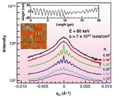 |
Fig. 96: Transverse GID curves perpendicular to the ripple structure around (220) Bragg peak of a ion-beam modified Si(001) wafer. Insets: AFM image (20 µm x 20 µm) and corresponding height profile. |
The Bragg intensity as a function of the incidence angle ai (Vineyard profiles) for samples bombarded with different dose are shown in Figure 97. The plateau below ![]() c, Si at about 0.23° (instead of a single peak at
c, Si at about 0.23° (instead of a single peak at ![]() i =
i = ![]() c, Si) seen here, corresponds to materials of low density, gradually decreasing towards the top. Since the measurements are on an in-plane Bragg peak, intensities at all incident angles stem from crystalline material. Note that the onset angle, the shape and height of the plateau are a function of the implantation dose. For low doses there are two distinct critical angles; the appearance of a peak at 0.05° is attributed to the existence of a partially crystalline top layer with much lower density compared to crystalline silicon. For increasing dose the intensity of the plateau-region decreases. In the case where the dose was 7x10¹⁷ ions/cm2, the plateau-region almost disappears and the shape of the
c, Si) seen here, corresponds to materials of low density, gradually decreasing towards the top. Since the measurements are on an in-plane Bragg peak, intensities at all incident angles stem from crystalline material. Note that the onset angle, the shape and height of the plateau are a function of the implantation dose. For low doses there are two distinct critical angles; the appearance of a peak at 0.05° is attributed to the existence of a partially crystalline top layer with much lower density compared to crystalline silicon. For increasing dose the intensity of the plateau-region decreases. In the case where the dose was 7x10¹⁷ ions/cm2, the plateau-region almost disappears and the shape of the ![]() i scan curve turns into a Vineyard profile expected for a sample with a non-scattering (amorphous) top layer. The reconstructed depth profile obtained from the simulation of the Vineyard profile (dotted lines in Figure 97) shows that the material density of the subsurface layer is very low (about 15% of the crystalline Si bulk density); at the same time the rippled, modulated crystalline part underneath is damaged and has a reduced density. The partially crystalline top layer at low dose, transforms to a completely amorphous layer for high doses and the surface morphology was found to be conformal with the underlying crystalline ripples.
i scan curve turns into a Vineyard profile expected for a sample with a non-scattering (amorphous) top layer. The reconstructed depth profile obtained from the simulation of the Vineyard profile (dotted lines in Figure 97) shows that the material density of the subsurface layer is very low (about 15% of the crystalline Si bulk density); at the same time the rippled, modulated crystalline part underneath is damaged and has a reduced density. The partially crystalline top layer at low dose, transforms to a completely amorphous layer for high doses and the surface morphology was found to be conformal with the underlying crystalline ripples.
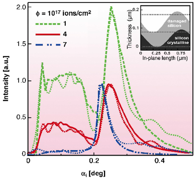 |
Fig. 97: Experimental and simulated (dotted) |
In conclusion, by a combination of GID and AFM measurements we have characterised the relation between the formation of ripple-like structure at the surface and the crystalline material in the subsurface region of the silicon wafer due to ion bombardment. The wavelength of the buried crystalline ripple structure is well replicated at the top surface as observed by AFM measurements.
References
[1] U. Valbusa, C. Boragno, and F.B. de Mongeot, J. Phys.: Condens. Matter 14, 8153 (2002).
[2] T.K. Chini, M.K. Sanyal, and S.R. Bhattacharyya, Phys. Rev. B 66, 153404 (2002).
Principal Publication and Authors
S. Hazra (a), T.K. Chini (a), M.K. Sanyal (a), J. Grenzer (b) and U. Pietsch (b), Phys. Rev. B 70, 121307 (2004), and H. Metzger (c).
(a) Saha Institute of Nuclear Physics, Kolkata (India)
(b) Institut fur Physik, Potsdam (Germany)
(c) ESRF
partners


European Synchrotron Radiation Facility - 71, avenue des Martyrs, CS 40220, 38043 Grenoble Cedex 9, France.