- Home
- Users & Science
- Scientific Documentation
- ESRF Highlights
- ESRF Highlights 2003
- Materials Science
- The Nanostructure Evolution During and After Magnetron Deposition of Au Films
The Nanostructure Evolution During and After Magnetron Deposition of Au Films
Nanocrystalline materials have unique properties and a great potential for industrial applications [1]. As the nanostructure strongly influences the physical and chemical properties, tailoring for specific applications requires an understanding of the mechanisms that control its formation and evolution. This is especially important as grain growth in nanocrystalline materials takes place at significantly lower temperatures than in coarser-grained materials, deteriorating the nanomaterial.
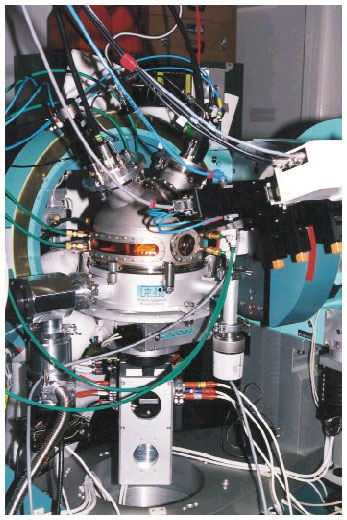
We chose magnetron sputtering as a versatile technique for deposition of thin-film nanocrystalline materials and gold as a model material (no oxidation) to study the formation and evolution of the nanostructure during growth and the evolution during thermal annealing after growth. The measurements were carried out in a deposition chamber, which was mounted on a six-circle goniometer at the ROBL (BM20) beamline (Figure 44). By in situ off-plane X-ray diffraction and in-plane Grazing-incidence X-ray Scattering (GIXS), the development of the preferred orientation of the grains, the lattice constant (stress), the grain size, and the microstrain were studied (the latter two by deconvolution of the diffraction profiles into Lorentzians and Gaussians).
 |
|
Fig. 44: Magnetron-sputter deposition chamber mounted on the six-circle diffractometer at ROBL. The vertical and horizontal X-ray windows allow a 3-dim. In situ characterisation of the structure and morphology of the growing film. |
With the deposition parameters chosen (1 inch Au target, dc power 10 W, base pressure 5 x 10⁻⁴ Pa, Ar 0.6 Pa during deposition at RT, Si(100)/a-SiO2 substrates mounted on a resistive heater, bias 30 V, growth rate 1.3 Å/s), Bragg-Brentano diffraction measurements revealed a dominating <111>-fibre texture, i.e. Au(111) lattice planes parallel to the film surface ((111) grains). Additionally, GIXS geometry identified (111)* grains (GIXS Au(111)) and (200)* grains (GIXS Au(200)), which were found to be more or less uniformly distributed throughout the film thickness. The (111) grains, on the contrary, were concentrated mainly in the upper part of the film.
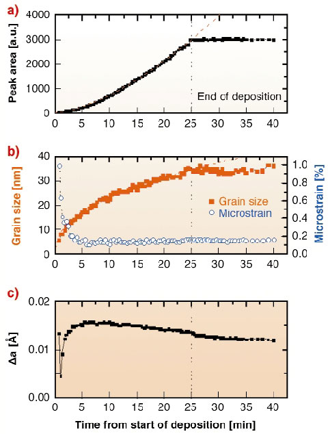
Figure 45 shows the typical growth behaviour. The initial, more-than-linear, increase in the Au(111) peak area with film thickness during deposition (Figure 45a) can be explained by a change of texture with time of growth and by an increase in (111) grains relative to (111)* grains during growth. Furthermore, during the initial growth, the microstrain dramatically decreased and the size of the coherently diffracting domains (equal to the grain size if the concentration of defects is sufficiently small) increased (Figure 45b). In the first minute of growth, the film stress decreased owing to a tensile contribution because of coalescence of initially-formed islands (Figure 45c).
 |
|
Fig. 45: The Bragg-Brentano Au(111) peak was measured as a function of deposition time during room temperature growth: (a) peak area (dashed line: power law fit); (b) microstrain and grain size (actually, the size of the coherently diffracting domains); (c) deviation of the lattice constant from the tabulated bulk value. |
During annealing at various temperatures, the Au(111) peak was similarly monitored. The microstrain rapidly decreased during the initial annealing, indicating annihilation of defects. At the same time, the coherently diffracting domains increased (with the activation energy of 0.25 ± 0.03 eV). Subsequently, normal grain growth was observed (activation energy 0.99 ± 0.04 eV).
Annealing revealed another interesting feature. Tilting the sample (with ![]() and 2
and 2![]() kept fixed at angles corresponding to standard Bragg-Brentano diffraction from Au(111) ) with the tilt axis lying at the intersection of the film surface and the scattering plane,
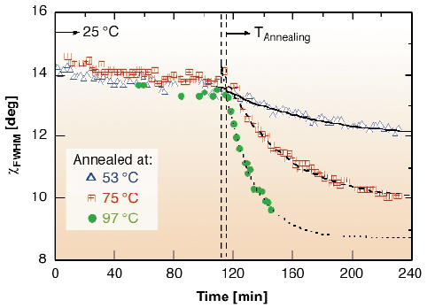
kept fixed at angles corresponding to standard Bragg-Brentano diffraction from Au(111) ) with the tilt axis lying at the intersection of the film surface and the scattering plane, ![]() -scans were made that yielded grain orientation distributions. The angular widths (FWHM) of these distributions were used as a measure of the texture. Figure 46 shows the typical behaviour of the measured widths. Such data together with the observation of the corresponding lack of grain growth lead to the interpretation that small rotations of individual grains with an activation energy of 0.64 ± 0.05 eV were responsible for the decrease in widths.
-scans were made that yielded grain orientation distributions. The angular widths (FWHM) of these distributions were used as a measure of the texture. Figure 46 shows the typical behaviour of the measured widths. Such data together with the observation of the corresponding lack of grain growth lead to the interpretation that small rotations of individual grains with an activation energy of 0.64 ± 0.05 eV were responsible for the decrease in widths.
 |
|
Fig. 46: FWHM of grain orientation distributions around the film-surface normal as a function of the time elapsed after the depositions stopped for various annealing temperatures. |
In conclusion, we could characterise the 3-dimensional evolution of the nanostructure of magnetron-sputtered nanocrystalline Au films during growth and subsequent annealing, and determine the mechanisms responsible with their corresponding activation energies, (defect annealing, grain rotations, normal grain growth and recrystallisation).
References:
[1] A.S. Edelstein, R.C. Cammarata (Eds.), Nanomaterials: Synthesis, Properties and Applications, Institute of Physics Publishing, Bristol (1998).
Principle Publication and Authors:
N. Schell (a, b), T. Jensen (c), J.H. Petersen (c), K.P. Andreasen (c), J. Bøttiger (c), J. Chevallier (c), Thin Solid Films 441, 96 (2003).
(a) Forschungszentrum Rossendorf, Dresden (Germany)
(b) ROBL-CRG, ESRF
(c) University of Aarhus (Denmark)
partners


European Synchrotron Radiation Facility - 71, avenue des Martyrs, CS 40220, 38043 Grenoble Cedex 9, France.