Figure 103
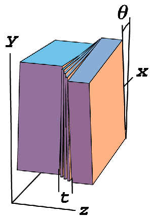
Fig. 103: Bonded crystals with twist angle ![]() have an interface with thickness t with modulated deformation.
have an interface with thickness t with modulated deformation.
| back to: The Interface Structure of Bonded Silicon Wafers |
partners


European Synchrotron Radiation Facility - 71, avenue des Martyrs, CS 40220, 38043 Grenoble Cedex 9, France.