- Home
- News
- Spotlight on Science
- Kinky copper: In...
Kinky copper: In situ X-ray characterisation of electrodeposited Cu on GaAs(001) reveals strange epitaxy
13-08-2007
A surface can be created with a unique morphology and structure on the mesoscopic and atomic scale by controlling the electrochemical potential via the voltage applied to the sample during the deposition of a metal from an electrolyte. This is important in electrochemical processing, for example for the formation of metallic interconnects in the next generation of nano-scale electronic devices. Electrodeposited Cu grows on GaAs(001) with an unusual structure: the nano-sized clusters are epitaxially rotated and tilted with respect to the support.
Atomic-scale structural characterisation of surfaces in contact with liquid electrolyte phases is a prerequisite for further understanding of systems important for many applications such as the Damascene process for the formation of metal interconnects in semiconductor devices, corrosion processes, and fuel cells. X-ray methods are uniquely suited to structural investigations in situ, in the presence of the electrolyte. However, preparing well-defined surfaces for electrochemical experiments in combination with in situ X-ray diffraction investigations is not trivial if the electrode surface under scrutiny is highly reactive. To date, only inert electrodes such as gold or platinum have been studied extensively.
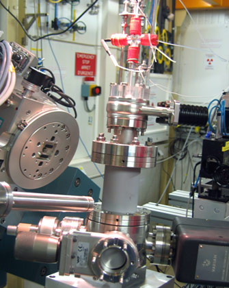 |
Figure 1: Photograph of the UHV chamber with electrochemical setup (top), mounted on the ID32 diffractometer. |
A new electrochemical setup has recently been commissioned at beamline ID32 [1] which consists of a miniature electrochemical cell with counter and reference electrode contained in a capillary, which is inserted into a portable ultra high vacuum (UHV) chamber (Figure 1) after this had been backfilled with inert gas. For the electrochemical experiments, contact with the sample surface is made with a droplet of electrolyte, formed at the tip of the capillary by the action of high resolution syringe pumps. The electrode potential is adjusted during in situ X-ray measurements by a computer controlled potentiostat.
The sample is prepared and characterised in a large UHV system in the ID32 surface characterisation laboratory and transferred into the portable chamber without exposure to ambient atmosphere. The specimen, with an ultra clean and well defined surface, can then be studied successively in UHV, in controlled gas atmospheres, and after insertion of the capillary into the chamber in contact with the electrolyte under applied potential.
 |
|
Figure 2: a) Reciprocal space map in the K,L-plane showing several Cu peaks originating from the "tilt" of the lattice planes of the Cu islands. b) Reciprocal space map in the H,K-plane showing the GaAs(020) peak and the ± 4.4 degree rotated Cu(020) peaks. c) Sequence of in-plane K-scans of a 2x4-reconstructed GaAs(001) surface in UHV, in N2 atmosphere at ambient pressure (middle) and in contact with 0.5 M H2SO4 + 1 mM CuSO4 solution at -100 mV. The peaks of the 2x4 reconstruction and of the epitaxial Cu are marked. The scattering background is enhanced by the gas and the liquid. |
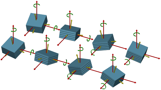
The setup was used to study the electro-deposition of copper from H2SO4:Cu on GaAs(001) surfaces (Figure 2). Atomically clean GaAs(001) surfaces had been prepared by molecular beam epitaxy and protected with 50 nm of amorphous As, this was carried out at the Norwegian University of Science and Technology in Trondheim. As and Ga terminated surfaces, and the corresponding reconstructed surfaces GaAs(001), were prepared in UHV in the surface characterisation laboratory of ID32 by desorption of the protective As layer. On such well defined As terminated surfaces, electrodeposited Cu was found to grow with "strange" epitaxial relations, with nanometre-sized islands exhibiting epitaxial rotation and, very unusual, epitaxial inclination by ± 4.4 degree and ± 8.8 degree, respectively (Figure 2). This results in a total of eight different type of Cu clusters with four different inclinations of the Cu(001) axis with respect to the GaAs(001) crystal axis, each combined with two in-plane rotations, as shown in Figure 3. Present research is focused on modifying the Cu structure and morphology by varying the applied potential and on understanding the origin of the strange epitaxy.
 |
|
Figure 3: Schematic real space representation of the eight possible rotated and tilted Cu domains. |
Reference
[1] F.U. Renner, Y. Gründer, J. Zegenhagen, Portable chamber for the study of UHV prepared electrochemical interfaces by hard X-ray diffraction, Rev. Sci. Instr. 78, 33903 (2007).
Authors
Y. Gründer (a), F.U. Renner (b), T-L. Lee (a), B.O. Fimland (c), J. Zegenhagen (a)
(a) ESRF
(b) AIST, Kansai-center, Ikeda (Japan)
(c) Norwegian University of Science and Technology, Trondheim (Norway)
partners


European Synchrotron Radiation Facility - 71, avenue des Martyrs, CS 40220, 38043 Grenoble Cedex 9, France.