- Home
- Users & Science
- Scientific Documentation
- ESRF Highlights
- ESRF Highlights 2017
- Structure of materials
- Carbon nanotubes as templates for 1D nanostructures via a one-reaction-one-pot method
Carbon nanotubes as templates for 1D nanostructures via a one-reaction-one-pot method
An all-in-one synthetic method has been developed, in which a single reactant, containing all the elements required for inorganic nanowires, is loaded into a carbon nanoreactor. Fluorescence-detected X-ray absorption and Raman spectroscopies in combination with transmission electron microscopy were used to monitor the transformations, revealing interactions between the nanotube and the molecules, stabilising the products.
Harnessing functional properties that emerge at the nanoscale is the key to developing superior materials for catalytic, electronic and biomedical applications. The internal cavity of single-walled carbon nanotubes (SWNTs) provides an effective template for control of the exact positions and orientations of molecules and atoms and has been successfully applied to the construction of nanoscale architectures from a variety of metals, [1,2] organic molecules, and inorganic compounds [1,2]. Low-dimensional inorganic materials, including transition metal chalcogenides, are of particular interest as their semiconducting properties can be precisely tuned by shaping their structures into nanoribbons. While the host nanotube can control the dimensions of the inorganic structure, the stoichiometry is much more difficult to control.
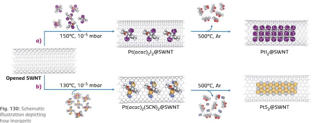
An all-in-one molecular precursor that contains all the necessary elements in the correct proportion for the desired inorganic product, encapsulated in SWNTs and subsequently converted into the inorganic material, offers a highly effective solution to this challenge. The one-pot-one-reactant synthesis involves a single step so that the stoichiometric ratio of the metal and halogen/chalcogen in the resultant material can be precisely controlled. The insertion of complexes of transition metals with ligands containing the required non-metallic elements into SWNTs is illustrated for platinum compounds containing Pt:I and Pt:S in ratios of 1:2 (Figure 130).
 |
|
Fig. 130: Schematic illustration depicting how inorganic nanomaterials, a) PtI2@SWNT; and b) PtS2@SWNT, can be formed using nanotubes as templates via a one-reactant-one-pot method. |
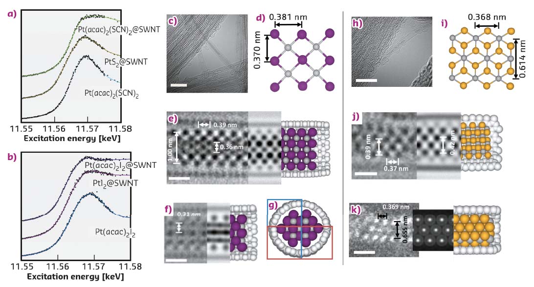
The L3 edge of Pt (measured in FD-XAS at BM28) can be used as a probe of the oxidation state of the species inside the nanotube and can thus elucidate any transfer of electron density to or from the reactant to the nanotube upon encapsulation. Furthermore, the characteristic G-band, ubiquitously observed in the Raman spectra of graphitic nanostructures, is sensitive to strain and curvature of the nanotube, and can be used to measure any electron transfer from the nanotube to guest molecules. Interestingly, the encapsulation of Pt(acac)2I2@SWNT led to a significant reduction in the absorption energy of the Pt L3 edge, indicative of an increase of electron density onto the Pt centre as compared to free Pt(acac)2I2, (Figure 131). This is complemented by a significant blue shift of the Raman G-band of the host SWNT, implying electron transfer from the nanotube to the guest molecule. In contrast, Pt(acac)2(SCN)2@SWNT showed a decrease in the Pt edge energy in the FD-XAS and a red shift of the nanotube G-band, indicating that electron density is transferred in the opposite direction, i.e. from Pt(acac)2(SCN)2 to SWNTs. Thermal treatment led to the facile transformation of the molecular precursors to the desired inorganic structures, PtI2@SWNT or PtS2@SWNT, with a nearly 1:2 stoichiometric metal to halogen/chalcogen composition and nanowire morphology.
 |
|
Fig. 131: a) and b) FD-XAS showing the Pt L3 edge of materials formed in SWNTs. c) AC-HRTEM image showing a bundle of PtI2@SWNT, the scale bar is 5 nm; d) an extended portion of the crystal structure of PtI2 derived from the asymmetric unit of bulk PtI2; e,f,g) two AC-HRTEM micrographs showing PtI2@SWNT in different projections, accompanying HR-TEM simulations and computational models, the scale bars are 0.5 nm; h) an AC-HRTEM micrograph showing a bundle of nanotubes containing PtS2 material, the scale bar is 5 nm; i) a portion of the crystal structure of bulk PtS2; j) an AC-HRTEM image of PtS2@SWNT with accompanying simulation and model, the scale bar is 0.5 nm; k) a HAADF-AC-STEM image PtS2@SWNT, with accompanying simulation and model. |
AC-HRTEM imaging reveals that the atomic level structure of the PtI2@SWNT is different to that of the bulk (Figure 131), with high-coordinated I-atoms in the middle of the structure and low-coordinated I atoms located in the space between the Pt and the SWNT wall, despite the overall Pt:I ratio being the same as in the bulk crystal. Such structural changes are a result of the confined monoclinic lattice adapting to the cylindrical channel of the SWNT to maximise van der Waals interactions. In contrast, in PtS2@SWNT the nanowire adopts a hexagonal lattice similar to bulk PtS2.
Principal publication and authors
A One-Pot-One-Reactant Synthesis of Platinum Compounds at the Nanoscale, C.T. Stoppiello (a), J. Biskupek (b), Z.Y. Li (c), G.A. Rance (a, d), A. Botos (a), R.M. Fogarty (e), R.A. Bourne (f), J. Yuan (g), K.R.J. Lovelock (h), P. Thompson (i, j), M.W. Fay (d), U. Kaiser (b), T.W. Chamberlain (f) and A.N. Khlobystov (a, d), Nanoscale 9, 14385-14394 (2017); doi: 10.1039/c7nr05976k.
(a) School of Chemistry, University of Nottingham (UK)
(b) Central Facility for Electron Microscopy, Ulm University (Germany)
(c) Nanoscale Physics Research Laboratory, School of Physics and Astronomy, University of Birmingham (UK)
(d) The Nanoscale and Microscale Research Centre, University of Nottingham (UK)
(e) Department of Chemistry, Imperial College London (UK)
(f) iPRD, School of Chemistry, University of Leeds (UK)
(g) Department of Physics, University of York (UK)
(h) Inorganic Chemistry Laboratory, University of Oxford (UK)
(i) Department of Physics, University of Liverpool (UK)
(j) ESRF
References
[1] T. Chamberlain et al., ACS Nano 11, 2509-2520 (2017).
[2] A. Botos et al., J. Am. Chem. Soc. 138, 8175-8183 (2016).
partners


European Synchrotron Radiation Facility - 71, avenue des Martyrs, CS 40220, 38043 Grenoble Cedex 9, France.