Figure 41
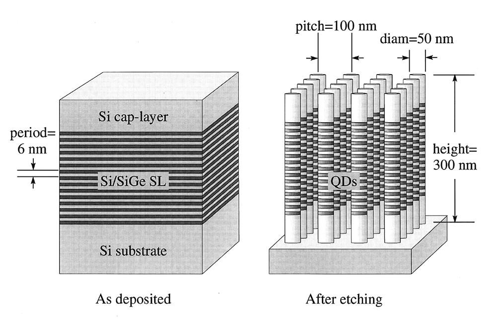
Fig. 41: A schematic view of the single crystal Si/SiGe structures. Left: the as-deposited strained layer superlattice (SL) with a periodicity of ~ 6 nm. Right: the array of quantum dots (QDs) after electron beam lithography and subsequent reactive ion etching. The pillars containing the QDs are of ~ 300 nm height and ~ 50 nm width with a pitch of 100 nm.
partners


European Synchrotron Radiation Facility - 71, avenue des Martyrs, CS 40220, 38043 Grenoble Cedex 9, France.