- Home
- Users & Science
- Scientific Documentation
- ESRF Highlights
- ESRF Highlights 2004
- X-ray Imaging
- Roughness Conformity during Tungsten Film Growth: An in situ Synchrotron X-ray Scattering Study
Roughness Conformity during Tungsten Film Growth: An in situ Synchrotron X-ray Scattering Study
Artificial thin films and layered systems are widely used in the fields of materials science, microelectronics and optics. They are also extensively employed in reflective synchrotron X-ray optics to tailor their optical properties. When diffraction-limited performance is desired, the most important surface parameters to be optimised are the figure and finish of the optics. While the desired optical figure can be reached via specific techniques, such as diamond turning, dynamical shaping or differential coating methods, the finish demands a control of the surfacing at the atomic level. Therefore, it is essential to understand the fundamental roughening and smoothing mechanisms that occur during mirror coating process.
Studies on thin film growth are frequently performed by interruption of the process followed by ex situ characterisation using either X-ray scattering techniques (XRS) or local probe techniques such as AFM or STM. In contrast, with grazing incidence XRS (GIXRS) techniques, measurements can be acquired in situ and in real-time, thus eliminating possible artifacts of the latter methods. Moreover, GIXRS method gives the unique possibility to investigate buried interfaces and to establish the degree of vertical correlation (conformity) between the roughness of the substrate and of the external film surface. Differentiating features induced by the topography of the substrate from those generated during deposition is an important asset in the optimisation of a growth process. Hence, an instrument capable of performing time-resolved reflectometry measurements on thin films has been developed [1].
In standard XRS data analysis [2, 3], based on the DWBA formalism, the relationship between the correlation functions due to the roughness at the various film interfaces and the scattering diagram is contained in an integral equation, so that the form of the autocorrelation function at each interface as well as the cross-correlation function must be postulated. In contrast, recent results obtained at the BM05 beamline show that, in the smooth surface limit[4], the general evolution of the roughness can be described in terms of its power spectrum density (PSD) without any model of film growth and/or correlation function (Figure 145a). From a direct evaluation of the PSD the roughness conformity was quantified using a replication factor defined as
K(p,h) = PSDsf(p,h) / ![]() PSDf(p,h)
PSDf(p,h)![]() PSDs(p).
PSDs(p).
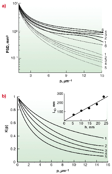 |
Fig. 145: (a): PSD-functions of the external film surface (solid curves) and of cross-correlation (dotted curves) extracted from the measured scattering diagrams as a function of the film thickness h (h = 5.6 nm (1), 10.2 nm (2), 14.8 nm (3), 19.4 nm (4), and 23.5 nm (5)). Curve 6 is the PSD-function of the silicon substrate. (b): Replication factor of roughness as a function of the film thickness). The inset shows the dependence of the characteristic length of roughness on the film thickness. |
The evolution of K(p) as a function of the film thickness h in the case of tungsten growth by sputtering deposition is presented in Figure 145b. The results enabled a quantitative estimation of the degree of conformity arising during film deposition and the determination of a characteristic wavelength Lc defined as the spatial dimension for which the replication factor would decrease by a factor e. The inset in Figure 145b shows the evolution of Lc as a function of the film thickness. After deposition of a film of thickness h features with a lateral size greater than Lc will be correctly replicated while additional uncorrelated roughness increases at decreasing spatial scale. For the tungsten growth process presented here, the critical size of a replicated feature would increase proportionally to the film thickness and the replication would only occur for surface features with a lateral size about 10 times greater than the film thickness could be correctly replicated.
The in situ XRS technique and data treatment presented here are expected to bring new insights in the comprehension of a large variety of processes, including sputter growth, evaporation, ion erosion and ion beam assisted deposition.
References
[1] L. Peverini, T. Bigault, and E. Ziegler, A real time in-situ X-ray scattering apparatus to monitor surface roughness. in Seventh Conference on the Physics of X-ray Multilayer Structures, Sapporo, Japan (2004).
[2] M. Tolan, X-ray scattering from soft-matter thin films : materials science and basic research. Springer tracts in modern physics ; 148. Berlin ; London: Springer. viii, 197 (1999).
[3] V. Holy, U. Pietsch, and T. Baumbach, High-resolution X-ray scattering from thin films and multilayers. Springer tracts in modern physics ; 149. Berlin ; New York: Springer. xi, 256 (1999).
[4] I.V. Kozhevnikov, Journal of X-ray Science and Technology 8, 253-275 (2000).
Principal Publications and Authors
L. Peverini (a), T. Bigault (b), I. V. Kozhevnikov (c) and E. Ziegler (a), submitted.
(a) ESRF
(b) ILL
(c) Institute of Crystallography, Moscow (Russia)
partners


European Synchrotron Radiation Facility - 71, avenue des Martyrs, CS 40220, 38043 Grenoble Cedex 9, France.