- Home
- Users & Science
- Scientific Documentation
- ESRF Highlights
- ESRF Highlights 2006
- Surface and Interface Science
- Implantation-induced crystalline defects in silicon studied by grazing incidence diffuse X-ray scattering
Implantation-induced crystalline defects in silicon studied by grazing incidence diffuse X-ray scattering
In the fabrication of CMOS devices, successive ion implantation and thermal annealing processing is employed. Increasing device performance is achieved by continuous shrinking of feature sizes. Therefore, front-end processors require an extremely accurate tailoring of the dopant profile especially close to the channel region, where ultra-shallow junctions are located with a junction depth lower than 50 nm. Industrially, ultra-shallow junctions are created by ultra-low energy (< 5 keV) implantation. Pre-amorphised Si substrates are often used to improve control of the dopant profile by avoiding ion-channelling. Understanding the mechanisms of dopant interaction with unavoidable implantation-induced defects has become a crucial issue.
The effects of pre-amorphisation on residual defects, especially end-of-range defects consisting of excess Si-interstitials [1], were investigated by focussing on two substrate series: pre-amorphised Si wafers (![]() -Si series) and untreated Si wafers (c-Si series). The
-Si series) and untreated Si wafers (c-Si series). The ![]() -Si substrates had been amorphised with Xe ions at 130 keV. Subsequently, As+ ions were implanted at 3 keV in all wafers to generate the ultra-shallow dopant profile. The As-implantation was followed by a treatment at 600°C for 20 minutes or by spike annealing at 1130°C, close to the processing conditions for industrial devices.
-Si substrates had been amorphised with Xe ions at 130 keV. Subsequently, As+ ions were implanted at 3 keV in all wafers to generate the ultra-shallow dopant profile. The As-implantation was followed by a treatment at 600°C for 20 minutes or by spike annealing at 1130°C, close to the processing conditions for industrial devices.
X-ray scattering experiments were carried out using an 8 keV beam at the beamline ID01. A combination of X-ray scattering methods optimised to characterise Si wafers implanted at ultra-low energy [2] was used. Grazing incidence diffuse X-ray scattering (GI-DXS) proved to be well suited to the investigation of defects confined within thin crystalline layers. The 220 surface Bragg reflection was selected and the X-ray grazing incident angle ![]() i was tuned to reach the depth where the defects are located. Reciprocal space maps in the (1
i was tuned to reach the depth where the defects are located. Reciprocal space maps in the (1![]() 0) plane (i.e. qr vs. qz) were recorded using a linear position sensitive detector.
0) plane (i.e. qr vs. qz) were recorded using a linear position sensitive detector.
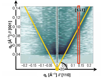
The analysis of the decay of the defect-induced DXS along q reveals information on the nature of the predominant defect. As expected for point defects and small defect clusters, a q-2 decay of the scattered intensity and a linear dependence from the defect concentration are found. For the c-Si samples, the intensity of the DXS progressively diminishes with increased annealing time, thus indicating the gradual annihilation of the defects. For spike-annealed ![]() -Si, the transformation of point defects into faulted dislocation loops was observed. These extended defects were identified from the DXS intensity streaks along the <111> directions, which are their characteristic “footprint” (Figure 88). All residual interstitials are condensed into loops with a diameter of ~ 50 nm measured from the width of the corresponding DXS streak.
-Si, the transformation of point defects into faulted dislocation loops was observed. These extended defects were identified from the DXS intensity streaks along the <111> directions, which are their characteristic “footprint” (Figure 88). All residual interstitials are condensed into loops with a diameter of ~ 50 nm measured from the width of the corresponding DXS streak.
 |
|
Fig. 88: Reciprocal space map of DXS in the qr-qz plane close to the 220 Bragg reflection for spike-annealed |
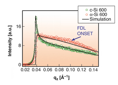
For small defects (i.e. q-2 decay of the DXS), it is possible to extract the depth profile of the defects by simulating the corresponding qz-resolved measurements. Figure 89 shows the quality of the fit performed using the program developed in [2]. The main information obtained is the value of the mean depth of the defects zmax where zmax = 12.5 ± 1 nm, for c-Si 600, and zmax = 100 ± 20 nm, for ![]() -Si 600, in agreement with the outcome of TEM and MEIS and TRIM calculations.
-Si 600, in agreement with the outcome of TEM and MEIS and TRIM calculations.
 |
|
Fig. 89: Defect-induced diffuse intensity along qz at qr = 0.14 Å-1 for |
The results obtained differ significantly between the two sample series and are compatible with the ‘excess interstitial’ model [1]. The distance of the defects from the sample surface is one of the key parameters which determine their evolution. In the ![]() -Si series, the end-of-range defects are deeply buried after Xe implantation. Therefore, they evolve from point-like into extended defects during annealing without losing Si interstitials. Due to the shallow location of the end-of-range damage, for c-Si implants, defect annihilation occurs by migration of Si interstitials towards the surface.
-Si series, the end-of-range defects are deeply buried after Xe implantation. Therefore, they evolve from point-like into extended defects during annealing without losing Si interstitials. Due to the shallow location of the end-of-range damage, for c-Si implants, defect annihilation occurs by migration of Si interstitials towards the surface.
These X-ray techniques offer a non-destructive tool for defect characterisation with high statistical accuracy, depth resolution and without the need for sample preparation.
References
[1] A. Claverie, B. Colombeau, B. De Maudit, C. Bonafos, X. Hebras, G. Ben Assayag, F. Cristiano, Appl. Phys. A 75, 1025 (2003).
[2] L. Capello, T.H. Metzger, V. Holy, M. Servidori, A. Malachias, J. Appl. Cryst. 39, 517 (2006).
Principal Publication and Authors
L. Capello (a), T.H. Metzger (a), M. Werner, J. van den Berg (b), M. Servidori (c), L. Ottaviano, C. Bongiorno, G. Mannino (d), T. Feudel, M. Herden (e), V. Holy (f), J. Appl. Phys. 100, 103533 (2006).
(a) ESRF
(b) University of Salford, (UK)
(c) CNR-IMM, Bologna, (Italy)
(d) CNR-IMM, Catania (Italy)
(e) AMD Saxony, Dresden (Germany)
(f) Charles University, Praha (Czech Republic)
partners


European Synchrotron Radiation Facility - 71, avenue des Martyrs, CS 40220, 38043 Grenoble Cedex 9, France.