- Home
- Users & Science
- Scientific Documentation
- ESRF Highlights
- ESRF Highlights 2001
- Micro-analysis and Imaging
- In situ Imaging of Misfit Dislocations during Relaxation Processes in Compound Semiconductor Epitaxial Layers
In situ Imaging of Misfit Dislocations during Relaxation Processes in Compound Semiconductor Epitaxial Layers
The molecular beam epitaxy reactor installed on beamline BM5 has been used to perform in situ high-resolution double axis X-ray diffraction topography (imaging) and diffraction measurements on strained layers of the compound semiconductor InxGa1-xAs grown epitaxially on the (001) surface of GaAs. Opto-electronic and high-speed devices based on such materials must operate reliably over extended periods and this means that the strained layer must not relax by creation of misfit dislocations at the interface. Experiments conducted at the ESRF have shed new light on the mechanisms by which such relaxation occurs.
New experiments on Si doped layers have identified the limits to which a modified Matthews and Blakeslee model, incorporating Peierls stress and impurity pinning, is applicable. For the fast B(g) dislocations, running in the [110] direction, and nucleated at regions of damage at the edges of the very low threading dislocation density, vertical gradient freeze GaAs substrates, the model holds well up to a Si concentration of 5 x 10118 cm-3 The critical thickness for misfit dislocation nucleation rises monotonically with Si concentration. For the slow A(g) set, running in the orthogonal [1![]() 0] direction, the model breaks down above a Si concentration of 2 x 018 cm-3, the critical thickness then becoming almost independent of dopant concentration. The deviation from the model occurs at a Si concentration at which cross-slip is observed to occur in the nucleation of the A(g) dislocations (Figure 136). In undoped layers and those with low Si concentration, no evidence of cross-slip was found.
0] direction, the model breaks down above a Si concentration of 2 x 018 cm-3, the critical thickness then becoming almost independent of dopant concentration. The deviation from the model occurs at a Si concentration at which cross-slip is observed to occur in the nucleation of the A(g) dislocations (Figure 136). In undoped layers and those with low Si concentration, no evidence of cross-slip was found.
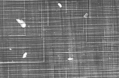 |
Fig. 136: Double axis in situ X-ray topograph showing evidence of cross slip occurring during nucleation of slow A(g) misfit dislocations at high Si dopant concentration. |
For undoped layers, only a very small change was observed in the critical thickness as a function of growth temperature. Inclusion of a temperature dependent term in the Matthews-Blakeslee model yielded an activation energy of 0.3 ± 0.2 eV. A larger drop in critical thickness with increasing growth temperature was observed in doped layers and the activation energy for the various relaxation processes observed in doped layers can be determined.
By measuring the intensity integrated over the image under fixed setting of beam-conditioning optics, it has been possible to observe for the first time the hardening of epilayers during relaxation. This measurement provides a measure of the radius of curvature of the wafer, which is proportional to the strain in the epilayer. Figure 137 shows the integrated intensity across the topographic image, as a function of thickness during the growth of an epitaxial layer. In the elastic region, the first of three stages visible, little or no relaxation occurs and the rate of increase of wafer curvature is high. In stage 1, equivalent to the region of easy glide in bulk systems, misfit dislocations are created freely and these are sufficiently mobile to relax all the additional strain introduced. There is no increase in wafer curvature. In stage 2, the lattice is hardened by interaction of the A(g) and B(g) dislocation sets and misfit dislocation motion is impeded. As a result substantial strain is locked into the layer and the curvature increases, but at a slower rate than in the elastic region. In situ rocking curve measurements, revealing incomplete relaxation in stage 2, confirm the analysis.
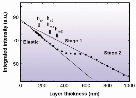 |
Fig. 137: Plot of integrated intensity across the topograph image versus epitaxial layer thickness for an In0.04Ga0.96As layer doped with 3.5 x 1018 cm-3 of Si. hc1, hc2, hm1, hm2 corresponding to the critical thickness for nucleation and multiplication of B(g) and A(g) misfit dislocations determined directly from the X-ray topographs. |
Principal Publication and Authors
B.K. Tanner (a), P.J. Parbrook (b), C.R. Whitehouse (b), A.M. Keir (c), A.D. John-son (c), J. Jones (c), D. Wallis (c), L.M. Smith (c), B. Lunn (d) and J.H.C. Hogg (e), J Phys D: Appl. Phys. 34, A109-A113 (2001)
(a) Dept. of Physics, University of Durham (UK)
(b) Dept. of Electrical and Electronic Engineering, University of Sheffield (UK)
(c) DERA, Great Malvern, (UK)
(d) School of Engineering, University of Hull (UK)
(e) Dept. of Physics, University of Hull (UK)
partners


European Synchrotron Radiation Facility - 71, avenue des Martyrs, CS 40220, 38043 Grenoble Cedex 9, France.