- Home
- Users & Science
- Scientific Documentation
- ESRF Highlights
- ESRF Highlights 2001
- Applied and Industrial Research
- Structural Defects in SiC Schottky Diodes
Structural Defects in SiC Schottky Diodes
Thanks to its excellent thermal, mechanical and electronic properties such as large band gap and high mobility, 4H silicon carbide (4H-SiC) is an important semiconductor for high-temperature, high-power and high-frequency devices. The behaviour of SiC devices depends on the structural quality and purity of the substrate, and on the device processing. Structural defects in SiC crystals are misoriented domains, inclusions, macrodefects, dislocations and micropipes [1]. X-ray topographic investigations were performed in order to separate and identify defects already present in the substrate and those induced during processing of Schottky diodes.
An n-type 6 µm thick epilayer with about 1016 cm-3 doping was grown using the CVD technique at about 1450°C on the front side of a 35 mm 4H-SiC 8° off axis wafer, 0.5 mm thick, purchased from CREE. Titanium was deposited as Schottky metal on top of the epilayer, and patterned, to make diodes with surface ranging from 0.1 to 2.3 mm2. The ohmic contact was obtained at the backside of the substrate, with a full sheet metallisation, and subsequent annealing. The synchrotron topography (diffraction imaging) was performed at the ID19 and BM5 beamlines.
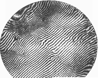 |
Fig. 152: "Zebra" pattern recorded on a non-processed SiC wafer (35 mm diameter), monochromatic beam with E = 18 keV used. The rotation step between consecutive exposures was 0.005°. |
Structural defects were investigated, on bare wafers, after epitaxy and after metallisation. The wafer curvature was examined using the so-called "zebra" pattern technique [2]. It consists of illuminating the crystal with a monochromatic beam and a step by step rocking of the sample around a given Bragg reflection peak. Due to the narrow wavelength selected by the monochromator and the dispersive geometry used, only some regions of the crystal diffract at a fixed sample position. Figure 152 gives a typical example of the "zebra" pattern recorded on a non-processed wafer and indicates the non-homogeneity of the structural defect density over the wafer and the presence of residual stresses. The radius of the curvature of the wafer is approximately 6 m. The dislocation, micropipe and subgrain boundary densities were not modified with processing. A detailed analysis shows that Schottky process did not generate new structural defects. On the other hand, the wafer curvature was modified from 6 m to 50 m after epitaxy and 11 m after the metallisation. The first modification is induced by an annealing phenomenon during epitaxy. The second one is due to the residual stress after polishing the backside of the wafer. This step is necessary in order to obtain a good ohmic contact.
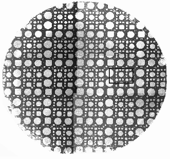 |
Fig. 153: Optical micrograph in reflection of a SiC wafer (35 mm diameter) with Schottky diodes. |
Figure 153 is an optical micrograph of a whole wafer with processed diodes. Figure 154 shows the 000l white beam back reflection topograph of a part of the wafer. The large white spots correspond to micropipes. The smaller spots are elementary screw dislocations. Each processed diode can be directly located on the topograph due to the stress introduced by the metal contacts. Diodes with or without defects have been selected in order to correlate the presence of defects with the electrical behaviour of the diodes.
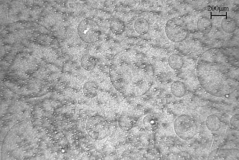 |
Fig. 154: White beam back reflection topograph of a part of the wafer shown in Figure 153. |
Schottky diodes were tested using an HP4156 Semiconductor Parameter Analyzer, by measuring I (V) characteristics in the forward and reverse mode. A correlation between the presence of subgrain boundary and leakage under low reverse voltage (20 V) was established. No influence of screw dislocations or micropipes was detected. A more detailed characterisation is underway, involving more devices and higher reverse voltages.
References
[1] R. Madar, M. Anikin, K. Chourou, M. Labeau, M. Pons, E. Blanquet, J.M. Dedulle, C. Bernard, S. Milita and J. Baruchel, Diamond and Related Materials, 6, 1249-1261 (1997).
[2] S. Kikuta, K. Kohra and Y. Sugita, Jap. J. of App. Phys., 5, 1047-1055 (1966).
Principal Publication and Authors
E. Pernot (a), E. Neyret (b), C. Moulin (b), P. Pernot-Rejmánková (c), F. Templier (b), L. Di Cioccio (b), T. Billon (b) and R. Madar (a), Material Science Forum, in press.
(a) LMGP-ENSPG, St Martin d'Hères (France)
(b) CEA/LETI, Grenoble (France)
(c) ESRF
partners


European Synchrotron Radiation Facility - 71, avenue des Martyrs, CS 40220, 38043 Grenoble Cedex 9, France.